
我是文本块。单击“编辑”按钮来更改此文本.
Introduction
Microfluidic chips manipulate trace biological samples through micron-scale precision microchannels, serving as core carriers for POCT in vitro diagnostics, cell sorting, and microscale biochemical experiments. Most academic laboratories still rely on manual single-chip prototyping, which cannot support mass commercial manufacturing. Combining real samples photographed on Suzhou Wenhao’s standardized mass production lines, this article fully breaks down the complete workflow: SU-8 photolithography master mold fabrication → replicated array substrate forming → bonding and packaging of finished chips. It covers both laboratory R&D and industrial mass manufacturing scenarios, analyzing mainstream microfluidic fabrication solutions objectively with all process samples captured on-site.
1. Figure 1: SU-8 Photolithography + Nickel Electroformed Master Mold – The Original Template for Microfluidic Mass Production
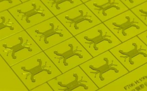
Many people confuse SU-8 photoresist masks with industrial metal master molds. The circular yellow wafer shown in the first image is the source template for the entire replication process.
Substrate Base & Photolithography Process
The base substrate is a 4/6-inch silicon wafer coated with thick-film negative SU-8 photoresist. After exposure and development via high-precision direct-write lithography equipment, raised “crab-shaped” microchannel positive molds are formed on the silicon wafer, with dimensional accuracy of ±1 μm, fully matching the design drawings of inertial focusing chips for cell sorting.
Nickel Electroforming to Extend Mass Production Lifespan
Pure SU-8 photoresist is brittle and cannot withstand high temperature and pressure, only supporting small-batch PDMS replication. For large-scale industrial manufacturing, a layer of metallic nickel is electroplated onto the SU-8 microstructures; after stripping, a metal positive mold (the raised metallic texture in the photo) is obtained.
- Advantages: High temperature resistance, wear resistance, capable of tens of thousands of PMMA hot embossing or injection molding cycles, eliminating the pain point of fragile photoresist molds unsuitable for industrialization.
- Mark Explanation: The marking “F706” at the bottom right of the wafer refers to the standardized chip model. This is a mass-produced inertial microfluidic chip mold developed by Suzhou Wenhao, applied to blood cell separation and microparticle screening.
Core Function of Master Molds
As a positive master template, all subsequent PDMS casting and plastic sheet hot embossing rely on this mold to replicate microchannel structures. The dimensional accuracy and consistency of all replicated parts are entirely determined by the master mold.
2. Figure 2: Replicated Array Substrates – Semi-Finished Boards with Mass-Replicated Microchannels
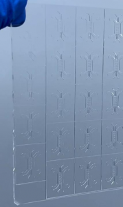
The transparent array sheet in the second photo is a semi-finished substrate replicated from the nickel master mold above. There are two mainstream material routes:
Route 1: Laboratory R&D – PDMS Cast Substrates
Liquid PDMS prepolymer is mixed with curing agent, evenly poured onto the nickel master mold, cured in a constant-temperature oven, then peeled off to obtain transparent PDMS sheets with recessed microchannels.
- Characteristics: Excellent light transmittance, favorable biocompatibility and elasticity, ideal for university lab research and short-term prototype verification.
- Limitations: High gas permeability, severe protein adsorption, incompatible with high-temperature sterilization, unsuitable for commercial mass production of in vitro diagnostic products.
Route 2: Industrial Mass Production – PMMA Hot Embossed Substrates (Mainstream Mass Production Solution of Suzhou Wenhao)
Optical-grade PMMA (acrylic) sheets are hot embossed under high temperature and pressure using the nickel master mold. Dozens of identical microchannel units can be formed on a single sheet in one process.
- Advantages: High rigidity, chemical inertness, resistance to reagent corrosion, low protein adsorption, suitable for high-volume cutting with far lower costs than PDMS, matching supporting chips for IVD diagnostic devices.
- Logic of Array Sheet Design: The array layout drastically boosts production efficiency, eliminating separate processing for individual chips. Independent single-chip substrates are obtained via laser cutting in the subsequent step.
The two types of substrates look visually similar, both featuring neatly arranged recessed microchannels as shown in the photo. Their differences lie only in material rigidity, chemical resistance and applicable scenarios.
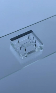
3. Figure 3: Bonding, Packaging & Port Machining – Finished Microfluidic Chips Ready for Instrument Testing
The independent transparent square chip in the third photo is a fully finished product after sheet cutting, sealing and fluid port machining, which can be directly connected to microfluidic pumps and valves for experiments.
3.1 Dicing & Cutting
The large array substrate in Figure 2 is divided into independent single-chip substrates via laser cutting or CNC milling.
3.2 Hermetic Bonding (Two Mature Processes)
- PDMS Solution: PDMS substrates and glass slides are treated with plasma cleaning, then irreversibly bonded to seal the bottom of microchannels and form closed fluid pipelines.
- PMMA Mass Production Solution: PMMA substrates are sealed with blank cover sheets via thermal bonding or solvent-assisted lamination, free of adhesive contamination for medical reagent detection applications.
3.3 Fluid Port Fabrication
The metal pins at the four corners of the chip serve as fluid inlets and outlets, corresponding to sample loading ports, buffer ports and waste liquid ports. Precision drilling and press-fitting of metal joints enable seamless connection with external tubing pumps to prevent liquid leakage and excessive dead volume.
3.4 Chip Function Introduction
This Model F706 inertial focusing microfluidic chip features an array of micro-pillars in the central zone. It separates cells and microparticles of different sizes based on fluid inertial force, widely used in circulating tumor cell isolation from peripheral blood, microsphere detection and research on microscale fluid dynamics.
4. Comparison of Two Mainstream Fabrication Routes (R&D vs Mass Production)
表格
| Fabrication Route | Core Master Mold | Substrate Material | Application Scenarios | Mass Production Capacity |
|---|---|---|---|---|
| Laboratory PDMS Route | SU-8 photoresist master mold / simplified nickel mold | Elastic PDMS gel | University research, prototype verification, short-term experiments | Small batch, dozens of chips per run |
| Industrial PMMA Hot Embossing Route | Nickel electroformed wafer master mold | Optical-grade PMMA | IVD diagnostics, supporting chips for commercial instruments | High volume, tens of thousands of chips per day |
Suzhou Wenhao covers both full-process production lines. We provide PDMS prototyping services for universities and research institutes, while owning complete production lines including nickel electroformed master mold fabrication, large-format PMMA hot embossing and automated bonding, balancing rapid R&D iteration and stable commercial bulk supply.
5. Clarification of Common Industry Process Misconceptions
Misconception 1: SU-8 photolithography molds can be directly used for mass production
Correction: Pure SU-8 photoresist cannot withstand the pressure of hot embossing and is only suitable for small-batch PDMS casting. Nickel electroforming reinforcement of the mold is mandatory for stable replication over tens of thousands of cycles.
Misconception 2: PDMS chips can be directly applied to commercial in vitro diagnostics
Correction: PDMS suffers from small molecule leaching, protein adsorption and vapor penetration. Hard plastics such as PMMA and COC are prioritized for compliant mass production of medical devices.
Misconception 3: CNC milled sheets deliver equivalent precision to hot embossed replicated molds
Correction: CNC milling has limits on minimum machining accuracy, with poor consistency for complex micron-scale micro-pillars and curved channels. Hot embossing replication via master molds delivers far superior uniformity and dimensional precision compared to mechanical milling.
Conclusion
The core bottleneck preventing microfluidic chips from laboratory to industrialization is not channel design, but standardized, highly consistent mass manufacturing processes. Every step from the original SU-8 photolithography master mold, through array replicated substrates, to fully packaged finished chips directly impacts experimental repeatability, mass production cost and regulatory compliance of chips.
If you have demands for microfluidic chip prototyping, mold development or bulk OEM manufacturing, feel free to discuss customized solutions tailored to your R&D or mass production needs.