I. selection of photoresist.
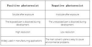
There are two basic types of photoresist: positive lithography and negative lithography, the difference is as follows

II. Lithography process steps.
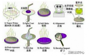
1. Clean silicon wafer.
Remove contaminants, impurities and particles by chemical cleaning, rinsing and drying to reduce pinholes and other defects to provide photoresist adhesion.
2. Pre-drying and bottom film coating.
Using HMDS as the primer, the-OH group on the surface of SiO2 can be removed, and the moisture on the wafer surface can be removed by dehydration and baking at 100C.
3. Photoresist coating.
The silicon wafer is placed on a high-speed rotating vacuum chuck, the liquid photoresist droplets are placed in the center of the wafer, and the photoresist expands outward by centrifugal force to spread evenly on the surface of the wafer.
4. Prebake.
Promote the full volatilization of the solvent in the film, make the film dry, and increase the adhesion and wear resistance to its SiO2. The baking time should not be too long and the temperature should not be too high.
5. Alignment.
In order to form a pattern on the silicon wafer successfully, the correct pattern on the silicon wafer must be aligned with the pattern on the mask. The registration accuracy is to measure the ability of the alignment system to engrave the layout onto the silicon wafer.
7.post exposure bake
The thermal motion of photoresist molecules occurs, and the overexposed and underexposed photoresist molecules are redistributed. Post-drying can balance the standing wave effect (interference between incident light and reflected light) and provide resolution.
8. Develop.
The purpose of dissolving the softened part of the photoresist is achieved by developing, rinsing and drying.
9. Hard film.
The temperature is usually 100-130 ℃ higher than the pre-drying temperature, and the time is 2 minutes. Evaporate all organic solvents in photoresist, improve resistance to etching and injection, improve photoresist and surface adhesion, polymerization and make photoresist more stable, photoresist flow to fill pinholes.
10. Graphic detection.
Through SEM, OM testing, if there are problems such as misalignment, mask rotation, wafer rotation, X-ray direction misalignment, critical size, surface irregularities (scratches, pinholes, defects and contaminants) need to peel off the photoresist and start over.

III. Wet etching.
1. When a material on the surface of silicon is dissolved in a chemical solution, the by-products are gases, liquids, or solids soluble in etching solutions.
2. The utility model has the advantages of simple process, good corrosion selectivity, serious drilling corrosion, poor precision and above 3um.
3. It is generally used to etch SiO2/Si/Poly-Si/Si3N4/Al2O3/TiO2.
IV. Dry etching.
1. Strong anisotropic corrosion, high resolution, can etch the lines below 3um.
2. Sputtering etching: the formation of high-energy plasma, bombarding the etched material, causing it to be spattered out by the hit atoms to form etching.
3. Plasma (Plasma) etching: plasma is produced. After glow discharge, the etching gas becomes a chemically active ion and free radical-plasma. The plasma active group reacts with the etched material.
4. Reactive ion etching (RIE): using both plasma etching and sputtering etching mechanisms, active ions plus ion bombardment.
